Skip to content
Gyanateet Dutta
Work·Academic·CV

Work

2026Systems

CUDA Blackwell Labs

Author, public repository

CUDA Blackwell Labs is a 22-project plan I worked through on an NVIDIA DGX Spark, whose GB10 chip shares 128 GB of memory between the CPU and the GPU. It runs from a hardware probe and memory microbenchmarks, through the CUDA-to-PTX-to-SASS pipeline, streams and CUDA Graphs, to hand-written FP16 and FP4 tensor-core instructions, TMA tile copies and a FlashAttention-style softmax. Sustained reads reached 231 GB/s, 85% of the 273 GB/s peak. Bandwidth fell from about 900 GB/s to DRAM speed once the working set outgrew the 24 MB L2 cache. cuBLAS ran a 4096 × 4096 GEMM at about 91 TFLOP/s in FP16, against 18 TFLOP/s in FP32.
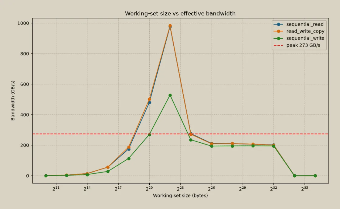
A line chart of effective bandwidth against working-set size, rising to about 980 GB/s at 4 MB, then falling to about 200 GB/s beyond the L2 cache, with a dashed line at the 273 GB/s peak.
Fig. 1Effective bandwidth by working-set size on the GB10, for sequential reads, writes and copies. Chart from Project 02 of Ryukijano/cuda-blackwell-labs, one run on one machine. Points above the dashed peak are served from the L2 cache; the two zero points are sizes the run did not record.
Scope

Every number is my own microbenchmark on one DGX Spark with CUDA 13. The GEMM figures are cuBLAS, not my kernels; my naive tensor-core kernel reached about 14 TFLOP/s.

Stack
CUDA 13, Blackwell, PTX, Tensor Cores
Links
Code

Also

  • 2026Agentic structure-from-motion
  • 2026PCOS edge agent
  • 2024Dalton Mills VR Reconstruction
  • 2023AWS AI/ML Scholar
  • B3tt3r: 3D Reconstruction
GitHub· ORCID· Google Scholar· LinkedIn· Hugging Face· X